-
The 3rd International Workshop on Overlay Architectures for FPGAs (OLAF 2017)
was held on 22 Feb, 2017 as a co-located workshop at the 25th ACM/SIGDA
International Symposium on Field-Programmable Gate Arrays (FPGA 2017). This
year, the program committee selected 3 papers and 3 extended abstracts to be
presented at the workshop, which are subsequently collected in this online
volume.
-
Static cache analysis characterizes a program's cache behavior by determining
in a sound but approximate manner which memory accesses result in cache hits
and which result in cache misses. Such information is valuable in optimizing
compilers, worst-case execution time analysis, and side-channel attack
quantification and mitigation.Cache analysis is usually performed as a
combination of `must' and `may' abstract interpretations, classifying
instructions as either `always hit', `always miss', or `unknown'. Instructions
classified as `unknown' might result in a hit or a miss depending on program
inputs or the initial cache state. It is equally possible that they do in fact
always hit or always miss, but the cache analysis is too coarse to see it.Our
approach to eliminate this uncertainty consists in (i) a novel abstract
interpretation able to ascertain that a particular instruction may definitely
cause a hit and a miss on different paths, and (ii) an exact analysis, removing
all remaining uncertainty, based on model checking, using
abstract-interpretation results to prune down the model for scalability.We
evaluated our approach on a variety of examples; it notably improves precision
upon classical abstract interpretation at reasonable cost.
-
An analog neural network computing engine based on CMOS-compatible
charge-trap transistor (CTT) is proposed in this paper. CTT devices are used as
analog multipliers. Compared to digital multipliers, CTT-based analog
multiplier shows significant area and power reduction. The proposed computing
engine is composed of a scalable CTT multiplier array and energy efficient
analog-digital interfaces. Through implementing the sequential analog fabric
(SAF), the engine mixed-signal interfaces are simplified and hardware overhead
remains constant regardless of the size of the array. A proof-of-concept 784 by
784 CTT computing engine is implemented using TSMC 28nm CMOS technology and
occupied 0.68mm2. The simulated performance achieves 76.8 TOPS (8-bit) with 500
MHz clock frequency and consumes 14.8 mW. As an example, we utilize this
computing engine to address a classic pattern recognition problem --
classifying handwritten digits on MNIST database and obtained a performance
comparable to state-of-the-art fully connected neural networks using 8-bit
fixed-point resolution.
-
We present a hardware mechanism called HourGlass to predictably share data in
a multi-core system where cores are explicitly designated as critical or
non-critical. HourGlass is a time-based cache coherence protocol for
dual-critical multi-core systems that ensures worst-case latency (WCL) bounds
for memory requests originating from critical cores. Although HourGlass does
not provide either WCL or bandwidth guarantees for memory requests from
non-critical cores, it promotes the use of timers to improve its bandwidth
utilization while still maintaining WCL bounds for critical cores. This
encourages a trade-off between the WCL bounds for critical cores, and the
improved memory bandwidth for non-critical cores via timer configurations. We
evaluate HourGlass using gem5, and with multithreaded benchmark suites
including SPLASH-2, and synthetic workloads. Our results show that the WCL for
critical cores with HourGlass is always within the analytical WCL bounds, and
provides a tighter WCL bound on critical cores compared to the state-of-the-art
real-time cache coherence protocol. Further, we show that HourGlass enables a
trade-off between provable WCL bounds for critical cores, and improved
bandwidth utilization for non-critical cores. The average-case performance of
HourGlass is comparable to the state-of-the-art real-time cache coherence
protocol, and suffers a slowdown of 1.43x and 1.46x compared to the
conventional MSI and MESI protocols.
-
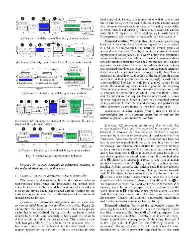
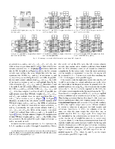
Loom (LM), a hardware inference accelerator for Convolutional Neural Networks
(CNNs) is presented. In LM every bit of data precision that can be saved
translates to proportional performance gains. Specifically, for convolutional
layers LM's execution time scales inversely proportionally with the precisions
of both weights and activations. For fully-connected layers LM's performance
scales inversely proportionally with the precision of the weights. LM targets
area- and bandwidth-constrained System-on-a-Chip designs such as those found on
mobile devices that cannot afford the multi-megabyte buffers that would be
needed to store each layer on-chip. Accordingly, given a data bandwidth budget,
LM boosts energy efficiency and performance over an equivalent bit-parallel
accelerator. For both weights and activations LM can exploit profile-derived
perlayer precisions. However, at runtime LM further trims activation precisions
at a much smaller than a layer granularity. Moreover, it can naturally exploit
weight precision variability at a smaller granularity than a layer. On average,
across several image classification CNNs and for a configuration that can
perform the equivalent of 128 16b x 16b multiply-accumulate operations per
cycle LM outperforms a state-of-the-art bit-parallel accelerator [1] by 4.38x
without any loss in accuracy while being 3.54x more energy efficient. LM can
trade-off accuracy for additional improvements in execution performance and
energy efficiency and compares favorably to an accelerator that targeted only
activation precisions. We also study 2- and 4-bit LM variants and find the the
2-bit per cycle variant is the most energy efficient.
-
With emerging storage-class memory (SCM) nearing commercialization, there is
evidence that it will deliver the much-anticipated high density and access
latencies within only a few factors of DRAM. Nevertheless, the
latency-sensitive nature of memory-resident services makes seamless integration
of SCM in servers questionable. In this paper, we ask the question of how best
to introduce SCM for such servers to improve overall performance/cost over
existing DRAM-only architectures. We first show that even with the most
optimistic latency projections for SCM, the higher memory access latency
results in prohibitive performance degradation. However, we find that
deployment of a modestly sized high-bandwidth 3D stacked DRAM cache makes the
performance of an SCM-mostly memory system competitive. The high degree of
spatial locality that memory-resident services exhibit not only simplifies the
DRAM cache's design as page-based, but also enables the amortization of
increased SCM access latencies and the mitigation of SCM's read/write latency
disparity.
We identify the set of memory hierarchy design parameters that plays a key
role in the performance and cost of a memory system combining an SCM technology
and a 3D stacked DRAM cache. We then introduce a methodology to drive
provisioning for each of these design parameters under a target
performance/cost goal. Finally, we use our methodology to derive concrete
results for specific SCM technologies. With PCM as a case study, we show that a
two bits/cell technology hits the performance/cost sweet spot, reducing the
memory subsystem cost by 40% while keeping performance within 3% of the best
performing DRAM-only system, whereas single-level and triple-level cell
organizations are impractical for use as memory replacements.
-
Advanced electronic device technologies require a faster operation and
smaller average power consumption, which are the most important parameters in
very large scale integrated circuit design. The conventional Complementary
Metal-Oxide Semiconductor (CMOS) technology is limited by the threshold voltage
and subthreshold leakage problems in scaling of devices. This leads to failure
in adapting it to sub-micron and nanotechnologies. The carbon nanotube (CNT)
technology overcomes the threshold voltage and subthreshold leakage problems
despite reduction in size. The CNT based technology develops the most promising
devices among emerging technologies because it has most of the desired
features. Carbon Nanotube Field Effect Transistors (CNFETs) are the novel
devices that are expected to sustain the transistor scalability while
increasing its performance. Recently, there have been tremendous advances in
CNT technology for nanoelectronics applications. CNFETs avoid most of the
fundamental limitations and offer several advantages compared to silicon-based
technology. Though CNT evolves as a better option to overcome some of the bulk
CMOS problems, the CNT itself still immersed with setbacks. The fabrication of
carbon nanotube at very large digital circuits on a single substrate is
difficult to achieve. Therefore, a hybrid NP dynamic Carry Look Ahead Adder
(CLA) is designed using p-CNFET and n-MOS transistors. Here, the performance of
CLA is evaluated in 8-bit, 16-bit, 32-bit and 64-bit stages with the following
four different implementations: silicon MOSFET (Si-MOSFET) domino logic,
Si-MOSFET NP dynamic CMOS, carbon nanotube MOSFET (CN-MOSFET) domino logic, and
CN-MOSFET NP dynamic CMOS. Finally, a Hybrid CMOS-CNFET based 64-bit NP dynamic
CLA is evaluated based on HSPICE simulation in 32nm technology, which
effectively suppresses power dissipation without an increase in propagation
delay.
-
Convolutional neural networks (CNNs) demonstrate excellent performance as
compared to conventional machine learning algorithms in various computer vision
applications. In recent years, FPGA-based CNN accelerators have been proposed
for optimizing performance and power efficiency. Most accelerators are designed
for object detection and recognition algorithms that are performed on
low-resolution (LR) images. However, image super-resolution (SR) cannot be
implemented in real time based on the typical accelerator because of the long
execution cycles required to generate high-resolution (HR) images, such as
those used in ultra-high-definition (UHD) systems. In this paper, we propose a
novel CNN accelerator with efficient parallelization methods for SR
applications. First, we propose a new methodology for optimizing the
deconvolutional neural networks (DCNNs) used for increasing feature maps, based
on trained filters. Second, we propose a novel method to optimize the CNN
dataflow using on-chip memory so that the SR algorithm can be driven at low
power in display applications. Third, we propose a two-stage quantization
algorithm to determine the optimized hardware size for a limited number of
DSPs. Finally, we present an energy-efficient architecture for SR and validate
our architecture on a mobile panel with quad-high-definition (QHD) resolution.
Our experimental results show that, with the same hardware resources, the
proposed DCNN accelerator achieves a throughput up to 108 times greater than
that of the conventional DCNN accelerator. In addition, our SR system achieves
an energy efficiency of 92.7 GOPS/W, 173.5 GOPS/W, and 286.8 GOPS/W when the
scale factors for SR are 2, 3, and 4, respectively. Furthermore, we demonstrate
that our system can restore HR images with a higher peak signal-to-noise-ratio
(PSNR) than conventional SR systems.
-
This book focuses on the use of algorithmic high-level synthesis (HLS) to
build application-specific FPGA systems. Our goal is to give the reader an
appreciation of the process of creating an optimized hardware design using HLS.
Although the details are, of necessity, different from parallel programming for
multicore processors or GPUs, many of the fundamental concepts are similar. For
example, designers must understand memory hierarchy and bandwidth, spatial and
temporal locality of reference, parallelism, and tradeoffs between computation
and storage. This book is a practical guide for anyone interested in building
FPGA systems. In a university environment, it is appropriate for advanced
undergraduate and graduate courses. At the same time, it is also useful for
practicing system designers and embedded programmers. The book assumes the
reader has a working knowledge of C/C++ and includes a significant amount of
sample code. In addition, we assume familiarity with basic computer
architecture concepts (pipelining, speedup, Amdahl's Law, etc.). A knowledge of
the RTL-based FPGA design flow is helpful, although not required.
-
This paper presents the Neural Cache architecture, which re-purposes cache
structures to transform them into massively parallel compute units capable of
running inferences for Deep Neural Networks. Techniques to do in-situ
arithmetic in SRAM arrays, create efficient data mapping and reducing data
movement are proposed. The Neural Cache architecture is capable of fully
executing convolutional, fully connected, and pooling layers in-cache. The
proposed architecture also supports quantization in-cache. Our experimental
results show that the proposed architecture can improve inference latency by
18.3x over state-of-art multi-core CPU (Xeon E5), 7.7x over server class GPU
(Titan Xp), for Inception v3 model. Neural Cache improves inference throughput
by 12.4x over CPU (2.2x over GPU), while reducing power consumption by 50% over
CPU (53% over GPU).
-
Energy efficiency and computing flexibility are some of the primary design
constraints of heterogeneous computing. In this paper, we present FlashAbacus,
a data-processing accelerator that self-governs heterogeneous kernel executions
and data storage accesses by integrating many flash modules in lightweight
multiprocessors. The proposed accelerator can simultaneously process data from
different applications with diverse types of operational functions, and it
allows multiple kernels to directly access flash without the assistance of a
host-level file system or an I/O runtime library. We prototype FlashAbacus on a
multicore-based PCIe platform that connects to FPGA-based flash controllers
with a 20 nm node process. The evaluation results show that FlashAbacus can
improve the bandwidth of data processing by 127%, while reducing energy
consumption by 78.4%, as compared to a conventional method of heterogeneous
computing. \blfootnote{This paper is accepted by and will be published at 2018
EuroSys. This document is presented to ensure timely dissemination of scholarly
and technical work.
-
This paper summarizes our work on experimentally characterizing, mitigating,
and recovering data retention errors in multi-level cell (MLC) NAND flash
memory, which was published in HPCA 2015, and examines the work's significance
and future potential. Retention errors, caused by charge leakage over time, are
the dominant source of flash memory errors. Understanding, characterizing, and
reducing retention errors can significantly improve NAND flash memory
reliability and endurance. In this work, we first characterize, with real 2Y-nm
MLC NAND flash chips, how the threshold voltage distribution of flash memory
changes with different retention ages -- the length of time since a flash cell
was programmed. We observe from our characterization results that 1) the
optimal read reference voltage of a flash cell, using which the data can be
read with the lowest raw bit error rate (RBER), systematically changes with its
retention age, and 2) different regions of flash memory can have different
retention ages, and hence different optimal read reference voltages.
Based on our findings, we propose two new techniques. First, Retention
Optimized Reading (ROR) adaptively learns and applies the optimal read
reference voltage for each flash memory block online. The key idea of ROR is to
periodically learn a tight upper bound of the optimal read reference voltage,
and from there approach the optimal read reference voltage. Our evaluations
show that ROR can extend flash memory lifetime by 64% and reduce average error
correction latency by 10.1%. Second, Retention Failure Recovery (RFR) recovers
data with uncorrectable errors offline by identifying and probabilistically
correcting flash cells with retention errors. Our evaluation shows that RFR
essentially doubles the error correction capability.
-
As the first kind of forward error correction (FEC) codes that achieve
channel capacity, polar codes have attracted much research interest recently.
Compared with other popular FEC codes, polar codes decoded by list successive
cancellation decoding (LSCD) with a large list size have better error
correction performance. However, due to the serial decoding nature of LSCD and
the high complexity of list management (LM), the decoding latency is high,
which limits the usage of polar codes in practical applications that require
low latency and high throughput. In this work, we study the high-throughput
implementation of LSCD with a large list size. Specifically, at the algorithmic
level, to achieve a low decoding latency with moderate hardware complexity, two
decoding schemes, a multi-bit double thresholding scheme and a partial G-node
look-ahead scheme, are proposed. Then, a high-throughput VLSI architecture
implementing the proposed algorithms is developed with optimizations on
different computation modules. From the implementation results on UMC 90 nm
CMOS technology, the proposed architecture achieves decoding throughputs of
1.103 Gbps, 977 Mbps and 827 Mbps when the list sizes are 8, 16 and 32,
respectively.
-
This article summarizes key results of our work on experimental
characterization and analysis of latency variation and latency-reliability
trade-offs in modern DRAM chips, which was published in SIGMETRICS 2016, and
examines the work's significance and future potential.
The goal of this work is to (i) experimentally characterize and understand
the latency variation across cells within a DRAM chip for these three
fundamental DRAM operations, and (ii) develop new mechanisms that exploit our
understanding of the latency variation to reliably improve performance. To this
end, we comprehensively characterize 240 DRAM chips from three major vendors,
and make six major new observations about latency variation within DRAM.
Notably, we find that (i) there is large latency variation across the cells for
each of the three operations; (ii) variation characteristics exhibit
significant spatial locality: slower cells are clustered in certain regions of
a DRAM chip; and (iii) the three fundamental operations exhibit different
reliability characteristics when the latency of each operation is reduced.
Based on our observations, we propose Flexible-LatencY DRAM (FLY-DRAM), a
mechanism that exploits latency variation across DRAM cells within a DRAM chip
to improve system performance. The key idea of FLY-DRAM is to exploit the
spatial locality of slower cells within DRAM, and access the faster DRAM
regions with reduced latencies for the fundamental operations. Our evaluations
show that FLY-DRAM improves the performance of a wide range of applications by
13.3%, 17.6%, and 19.5%, on average, for each of the three different vendors'
real DRAM chips, in a simulated 8-core system.
-
This paper summarizes our work on experimental characterization and analysis
of reduced-voltage operation in modern DRAM chips, which was published in
SIGMETRICS 2017, and examines the work's significance and future potential.
We take a comprehensive approach to understanding and exploiting the latency
and reliability characteristics of modern DRAM when the DRAM supply voltage is
lowered below the nominal voltage level specified by DRAM standards. We perform
an experimental study of 124 real DDR3L (low-voltage) DRAM chips manufactured
recently by three major DRAM vendors. We find that reducing the supply voltage
below a certain point introduces bit errors in the data, and we comprehensively
characterize the behavior of these errors. We discover that these errors can be
avoided by increasing the latency of three major DRAM operations (activation,
restoration, and precharge). We perform detailed DRAM circuit simulations to
validate and explain our experimental findings. We also characterize the
various relationships between reduced supply voltage and error locations,
stored data patterns, DRAM temperature, and data retention.
Based on our observations, we propose a new DRAM energy reduction mechanism,
called Voltron. The key idea of Voltron is to use a performance model to
determine by how much we can reduce the supply voltage without introducing
errors and without exceeding a user-specified threshold for performance loss.
Our evaluations show that Voltron reduces the average DRAM and system energy
consumption by 10.5% and 7.3%, respectively, while limiting the average system
performance loss to only 1.8%, for a variety of memory-intensive quad-core
workloads. We also show that Voltron significantly outperforms prior dynamic
voltage and frequency scaling mechanisms for DRAM.
-
This paper summarizes the idea of Low-Cost Interlinked Subarrays (LISA),
which was published in HPCA 2016, and examines the work's significance and
future potential. Contemporary systems perform bulk data movement movement
inefficiently, by transferring data from DRAM to the processor, and then back
to DRAM, across a narrow off-chip channel. The use of this narrow channel
results in high latency and energy consumption. Prior work proposes to avoid
these high costs by exploiting the existing wide internal DRAM bandwidth for
bulk data movement, but the limited connectivity of wires within DRAM allows
fast data movement within only a single DRAM subarray. Each subarray is only a
few megabytes in size, greatly restricting the range over which fast bulk data
movement can happen within DRAM.
Our HPCA 2016 paper proposes a new DRAM substrate, Low-Cost Inter-Linked
Subarrays (LISA), whose goal is to enable fast and efficient data movement
across a large range of memory at low cost. LISA adds low-cost connections
between adjacent subarrays. By using these connections to interconnect the
existing internal wires (bitlines) of adjacent subarrays, LISA enables
wide-bandwidth data transfer across multiple subarrays with little (only 0.8%)
DRAM area overhead. As a DRAM substrate, LISA is versatile, enabling a variety
of new applications. We describe and evaluate three such applications in
detail: (1) fast inter-subarray bulk data copy, (2) in-DRAM caching using a
DRAM architecture whose rows have heterogeneous access latencies, and (3)
accelerated bitline precharging by linking multiple precharge units together.
Our extensive evaluations show that each of LISA's three applications
significantly improves performance and memory energy efficiency on a variety of
workloads and system configurations.
-
This paper summarizes the SoftMC DRAM characterization infrastructure, which
was published in HPCA 2017, and examines the work's significance and future
potential.
SoftMC (Soft Memory Controller) is the first publicly-available DRAM testing
infrastructure that can flexibly and efficiently test DRAM chips in a manner
accessible to both software and hardware developers. SoftMC is an FPGA-based
testing platform that can control and test memory modules designed for the
commonly-used DDR (Double Data Rate) interface. SoftMC has two key properties:
(i) it provides flexibility to thoroughly control memory behavior or to
implement a wide range of mechanisms using DDR commands; and (ii) it is easy to
use as it provides a simple and intuitive high-level programming interface for
users, completely hiding the low-level details of the FPGA.
We demonstrate the capability, flexibility, and programming ease of SoftMC
with two example use cases. First, we implement a test that characterizes the
retention time of DRAM cells. Second, we show that the expected latency
reduction of two recently-proposed mechanisms, which rely on accessing
recently-refreshed or recently-accessed DRAM cells faster than other DRAM
cells, is not observable in existing DRAM chips.
Various versions of the SoftMC platform have enabled many of our other DRAM
characterization studies. We discuss several other use cases of SoftMC,
including the ability to characterize emerging non-volatile memory modules that
obey the DDR standard. We hope that our open-source release of SoftMC fills a
gap in the space of publicly-available experimental memory testing
infrastructures and inspires new studies, ideas, and methodologies in memory
system design.
-
This paper summarizes our work on experimentally characterizing, mitigating,
and recovering read disturb errors in multi-level cell (MLC) NAND flash memory,
which was published in DSN 2015, and examines the work's significance and
future potential. NAND flash memory reliability continues to degrade as the
memory is scaled down and more bits are programmed per cell. A key contributor
to this reduced reliability is read disturb, where a read to one row of cells
impacts the threshold voltages of unread flash cells in different rows of the
same block.
For the first time in open literature, this work experimentally characterizes
read disturb errors on state-of-the-art 2Y-nm (i.e., 20-24 nm) MLC NAND flash
memory chips. Our findings (1) correlate the magnitude of threshold voltage
shifts with read operation counts, (2) demonstrate how program/erase cycle
count and retention age affect the read-disturb-induced error rate, and (3)
identify that lowering pass-through voltage levels reduces the impact of read
disturb and extend flash lifetime. Particularly, we find that the probability
of read disturb errors increases with both higher wear-out and higher
pass-through voltage levels.
We leverage these findings to develop two new techniques. The first technique
mitigates read disturb errors by dynamically tuning the pass-through voltage on
a per-block basis. Using real workload traces, our evaluations show that this
technique increases flash memory endurance by an average of 21%. The second
technique recovers from previously-uncorrectable flash errors by identifying
and probabilistically correcting cells susceptible to read disturb errors. Our
evaluations show that this recovery technique reduces the raw bit error rate by
36%.
-
This paper summarizes our work on experimentally analyzing, exploiting, and
addressing vulnerabilities in multi-level cell NAND flash memory programming,
which was published in the industrial session of HPCA 2017, and examines the
work's significance and future potential. Modern NAND flash memory chips use
multi-level cells (MLC), which store two bits of data in each cell, to improve
chip density. As MLC NAND flash memory scaled down to smaller manufacturing
process technologies, manufacturers adopted a two-step programming method to
improve reliability. In two-step programming, the two bits of a multi-level
cell are programmed using two separate steps, in order to minimize the amount
of cell-to-cell program interference induced on neighboring flash cells.
In this work, we demonstrate that two-step programming exposes new
reliability and security vulnerabilities in state-of-the-art MLC NAND flash
memory. We experimentally characterize contemporary 1X-nm (i.e., 15--19nm)
flash memory chips, and find that a partially-programmed flash cell (i.e., a
cell where the second programming step has not yet been performed) is much more
vulnerable to cell-to-cell interference and read disturb than a
fully-programmed cell. We show that it is possible to exploit these
vulnerabilities on solid-state drives (SSDs) to alter the partially-programmed
data, causing (potentially malicious) data corruption. Based on our
observations, we propose several new mechanisms that eliminate or mitigate
these vulnerabilities in partially-programmed cells, and at the same time
increase flash memory lifetime by 16%.
-
This paper summarizes the idea of ChargeCache, which was published in HPCA
2016 [51], and examines the work's significance and future potential. DRAM
latency continues to be a critical bottleneck for system performance. In this
work, we develop a low-cost mechanism, called ChargeCache, that enables faster
access to recently-accessed rows in DRAM, with no modifications to DRAM chips.
Our mechanism is based on the key observation that a recently-accessed row has
more charge and thus the following access to the same row can be performed
faster. To exploit this observation, we propose to track the addresses of
recently-accessed rows in a table in the memory controller. If a later DRAM
request hits in that table, the memory controller uses lower timing parameters,
leading to reduced DRAM latency. Row addresses are removed from the table after
a specified duration to ensure rows that have leaked too much charge are not
accessed with lower latency. We evaluate ChargeCache on a wide variety of
workloads and show that it provides significant performance and energy benefits
for both single-core and multi-core systems.
-
This paper presents a survey of the currently available hardware designs for
implementation of the human cortex inspired algorithm, Hierarchical Temporal
Memory (HTM). In this review, we focus on the state of the art advances of
memristive HTM implementation and related HTM applications. With the advent of
edge computing, HTM can be a potential algorithm to implement on-chip near
sensor data processing. The comparison of analog memristive circuit
implementations with the digital and mixed-signal solutions are provided. The
advantages of memristive HTM over digital implementations against performance
metrics such as processing speed, reduced on-chip area and power dissipation
are discussed. The limitations and open problems concerning the memristive HTM,
such as the design scalability, sneak currents, leakage, parasitic effects,
lack of the analog learning circuits implementations and unreliability of the
memristive devices integrated with CMOS circuits are also discussed.
-
In existing systems, to perform any bulk data movement operation (copy or
initialization), the data has to first be read into the on-chip processor, all
the way into the L1 cache, and the result of the operation must be written back
to main memory. This is despite the fact that these operations do not involve
any actual computation. RowClone exploits the organization and operation of
commodity DRAM to perform these operations completely inside DRAM using two
mechanisms. The first mechanism, Fast Parallel Mode, copies data between two
rows inside the same DRAM subarray by issuing back-to-back activate commands to
the source and the destination row. The second mechanism, Pipelined Serial
Mode, transfers cache lines between two banks using the shared internal bus.
RowClone significantly reduces the raw latency and energy consumption of bulk
data copy and initialization. This reduction directly translates to improvement
in performance and energy efficiency of systems running copy or
initialization-intensive workloads
-
This paper summarizes the idea of Subarray-Level Parallelism (SALP) in DRAM,
which was published in ISCA 2012, and examines the work's significance and
future potential. Modern DRAMs have multiple banks to serve multiple memory
requests in parallel. However, when two requests go to the same bank, they have
to be served serially, exacerbating the high latency of on-chip memory. Adding
more banks to the system to mitigate this problem incurs high system cost. Our
goal in this work is to achieve the benefits of increasing the number of banks
with a low-cost approach. To this end, we propose three new mechanisms, SALP-1,
SALP-2, and MASA (Multitude of Activated Subarrays), to reduce the
serialization of different requests that go to the same bank. The key
observation exploited by our mechanisms is that a modern DRAM bank is
implemented as a collection of subarrays that operate largely independently
while sharing few global peripheral structures.
Our three proposed mechanisms mitigate the negative impact of bank
serialization by overlapping different components of the bank access latencies
of multiple requests that go to different subarrays within the same bank.
SALP-1 requires no changes to the existing DRAM structure, and needs to only
reinterpret some of the existing DRAM timing parameters. SALP-2 and MASA
require only modest changes (< 0.15% area overhead) to the DRAM peripheral
structures, which are much less design constrained than the DRAM core. Our
evaluations show that SALP-1, SALP-2 and MASA significantly improve performance
for both single-core systems (7%/13%/17%) and multi-core systems (15%/16%/20%),
averaged across a wide range of workloads. We also demonstrate that our
mechanisms can be combined with application-aware memory request scheduling in
multicore systems to further improve performance and fairness.
-
This paper summarizes the idea of Adaptive-Latency DRAM (AL-DRAM), which was
published in HPCA 2015, and examines the work's significance and future
potential. AL-DRAM is a mechanism that optimizes DRAM latency based on the DRAM
module and the operating temperature, by exploiting the extra margin that is
built into the DRAM timing parameters. DRAM manufacturers provide a large
margin for the timing parameters as a provision against two worst-case
scenarios. First, due to process variation, some outlier DRAM chips are much
slower than others. Second, chips become slower at higher temperatures. The
timing parameter margin ensures that the slow outlier chips operate reliably at
the worst-case temperature, and hence leads to a high access latency.
Using an FPGA-based DRAM testing platform, our work first characterizes the
extra margin for 115 DRAM modules from three major manufacturers. The
experimental results demonstrate that it is possible to reduce four of the most
critical timing parameters by a minimum/maximum of 17.3%/54.8% at 55C while
maintaining reliable operation. AL-DRAM uses these observations to adaptively
select reliable DRAM timing parameters for each DRAM module based on the
module's current operating conditions. AL-DRAM does not require any changes to
the DRAM chip or its interface; it only requires multiple different timing
parameters to be specified and supported by the memory controller. Our real
system evaluations show that AL-DRAM improves the performance of
memory-intensive workloads by an average of 14% without introducing any errors.
Our characterization and proposed techniques have inspired several other works
on analyzing and/or exploiting different sources of latency and performance
variation within DRAM chips.
-
This paper summarizes the idea of Tiered-Latency DRAM (TL-DRAM), which was
published in HPCA 2013, and examines the work's significance and future
potential. The capacity and cost-per-bit of DRAM have historically scaled to
satisfy the needs of increasingly large and complex computer systems. However,
DRAM latency has remained almost constant, making memory latency the
performance bottleneck in today's systems. We observe that the high access
latency is not intrinsic to DRAM, but a trade-off is made to decrease the cost
per bit. To mitigate the high area overhead of DRAM sensing structures,
commodity DRAMs connect many DRAM cells to each sense amplifier through a wire
called a bitline. These bit-lines have a high parasitic capacitance due to
their long length, and this bitline capacitance is the dominant source of DRAM
latency. Specialized low-latency DRAMs use shorter bitlines with fewer cells,
but have a higher cost-per-bit due to greater sense amplifier area overhead. To
achieve both low latency and low cost per bit, we introduce Tiered-Latency DRAM
(TL-DRAM). In TL-DRAM, each long bitline is split into two shorter segments by
an isolation transistor, allowing one of the two segments to be accessed with
the latency of a short-bitline DRAM without incurring a high cost per bit. We
propose mechanisms that use the low-latency segment as a hardware-managed or
software-managed cache. Our evaluations show that our proposed mechanisms
improve both performance and energy efficiency for both single-core and
multiprogrammed workloads. Tiered-Latency DRAM has inspired several other works
on reducing DRAM latency with little to no architectural modification.
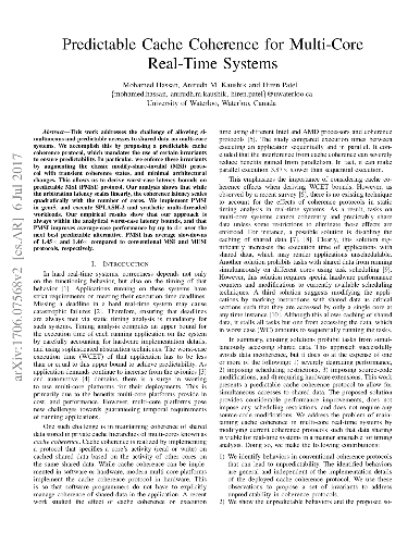
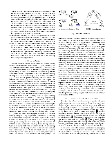
 We present a hardware mechanism called HourGlass to predictably share data in a multi-core system where cores are explicitly designated as critical or non-critical. HourGlass is a time-based cache coherence protocol for dual-critical multi-core systems that ensures worst-case latency (WCL) bounds for memory requests originating from critical cores. Although HourGlass does not provide either WCL or bandwidth guarantees for memory requests from non-critical cores, it promotes the use of timers to improve its bandwidth utilization while still maintaining WCL bounds for critical cores. This encourages a trade-off between the WCL bounds for critical cores, and the improved memory bandwidth for non-critical cores via timer configurations. We evaluate HourGlass using gem5, and with multithreaded benchmark suites including SPLASH-2, and synthetic workloads. Our results show that the WCL for critical cores with HourGlass is always within the analytical WCL bounds, and provides a tighter WCL bound on critical cores compared to the state-of-the-art real-time cache coherence protocol. Further, we show that HourGlass enables a trade-off between provable WCL bounds for critical cores, and improved bandwidth utilization for non-critical cores. The average-case performance of HourGlass is comparable to the state-of-the-art real-time cache coherence protocol, and suffers a slowdown of 1.43x and 1.46x compared to the conventional MSI and MESI protocols.
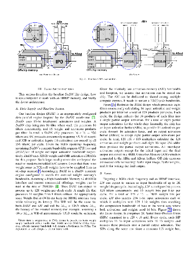
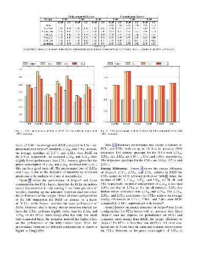 Loom (LM), a hardware inference accelerator for Convolutional Neural Networks (CNNs) is presented. In LM every bit of data precision that can be saved translates to proportional performance gains. Specifically, for convolutional layers LM's execution time scales inversely proportionally with the precisions of both weights and activations. For fully-connected layers LM's performance scales inversely proportionally with the precision of the weights. LM targets area- and bandwidth-constrained System-on-a-Chip designs such as those found on mobile devices that cannot afford the multi-megabyte buffers that would be needed to store each layer on-chip. Accordingly, given a data bandwidth budget, LM boosts energy efficiency and performance over an equivalent bit-parallel accelerator. For both weights and activations LM can exploit profile-derived perlayer precisions. However, at runtime LM further trims activation precisions at a much smaller than a layer granularity. Moreover, it can naturally exploit weight precision variability at a smaller granularity than a layer. On average, across several image classification CNNs and for a configuration that can perform the equivalent of 128 16b x 16b multiply-accumulate operations per cycle LM outperforms a state-of-the-art bit-parallel accelerator [1] by 4.38x without any loss in accuracy while being 3.54x more energy efficient. LM can trade-off accuracy for additional improvements in execution performance and energy efficiency and compares favorably to an accelerator that targeted only activation precisions. We also study 2- and 4-bit LM variants and find the the 2-bit per cycle variant is the most energy efficient.
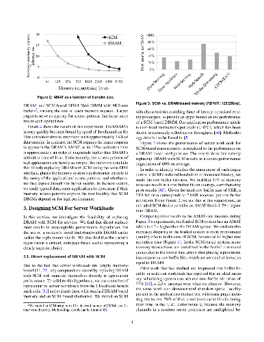
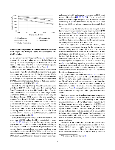
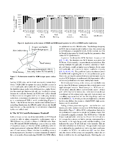 With emerging storage-class memory (SCM) nearing commercialization, there is evidence that it will deliver the much-anticipated high density and access latencies within only a few factors of DRAM. Nevertheless, the latency-sensitive nature of memory-resident services makes seamless integration of SCM in servers questionable. In this paper, we ask the question of how best to introduce SCM for such servers to improve overall performance/cost over existing DRAM-only architectures. We first show that even with the most optimistic latency projections for SCM, the higher memory access latency results in prohibitive performance degradation. However, we find that deployment of a modestly sized high-bandwidth 3D stacked DRAM cache makes the performance of an SCM-mostly memory system competitive. The high degree of spatial locality that memory-resident services exhibit not only simplifies the DRAM cache's design as page-based, but also enables the amortization of increased SCM access latencies and the mitigation of SCM's read/write latency disparity. We identify the set of memory hierarchy design parameters that plays a key role in the performance and cost of a memory system combining an SCM technology and a 3D stacked DRAM cache. We then introduce a methodology to drive provisioning for each of these design parameters under a target performance/cost goal. Finally, we use our methodology to derive concrete results for specific SCM technologies. With PCM as a case study, we show that a two bits/cell technology hits the performance/cost sweet spot, reducing the memory subsystem cost by 40% while keeping performance within 3% of the best performing DRAM-only system, whereas single-level and triple-level cell organizations are impractical for use as memory replacements.
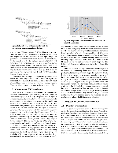
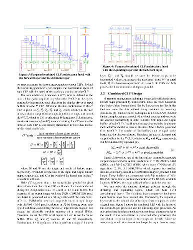
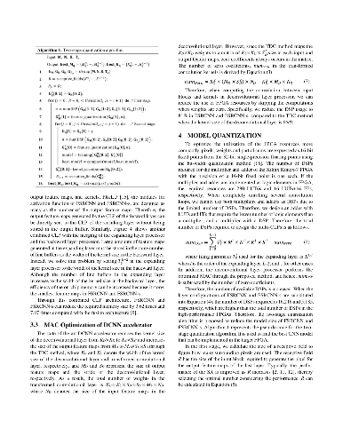
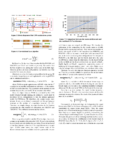
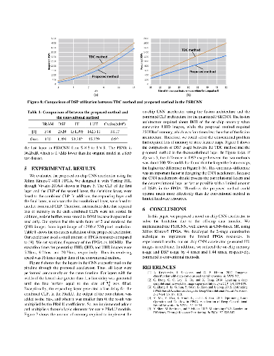 Convolutional neural networks (CNNs) demonstrate excellent performance as compared to conventional machine learning algorithms in various computer vision applications. In recent years, FPGA-based CNN accelerators have been proposed for optimizing performance and power efficiency. Most accelerators are designed for object detection and recognition algorithms that are performed on low-resolution (LR) images. However, image super-resolution (SR) cannot be implemented in real time based on the typical accelerator because of the long execution cycles required to generate high-resolution (HR) images, such as those used in ultra-high-definition (UHD) systems. In this paper, we propose a novel CNN accelerator with efficient parallelization methods for SR applications. First, we propose a new methodology for optimizing the deconvolutional neural networks (DCNNs) used for increasing feature maps, based on trained filters. Second, we propose a novel method to optimize the CNN dataflow using on-chip memory so that the SR algorithm can be driven at low power in display applications. Third, we propose a two-stage quantization algorithm to determine the optimized hardware size for a limited number of DSPs. Finally, we present an energy-efficient architecture for SR and validate our architecture on a mobile panel with quad-high-definition (QHD) resolution. Our experimental results show that, with the same hardware resources, the proposed DCNN accelerator achieves a throughput up to 108 times greater than that of the conventional DCNN accelerator. In addition, our SR system achieves an energy efficiency of 92.7 GOPS/W, 173.5 GOPS/W, and 286.8 GOPS/W when the scale factors for SR are 2, 3, and 4, respectively. Furthermore, we demonstrate that our system can restore HR images with a higher peak signal-to-noise-ratio (PSNR) than conventional SR systems.