-
Nowadays, a problem of historical beadworks conservation in museum
collections is actual more than ever because of fatal corrosion of the 19th
century glass beads. Vibrational spectroscopy is a powerful method for
investigation of glass, namely, of correlation of the structure-chemical
composition. Therefore, Fourier-transform infrared spectroscopy was used for
examination of degradation processes in cloudy turquoise glass beads, which in
contrast to other color ones deteriorate especially strongly. Micro-X-ray
fluorescence spectrometry of samples has shown that lead-potassium glass
PbO-K$_2$O-SiO$_2$ with small amount of Cu and Sb was used for manufacture of
cloudy turquoise beads. Fourier-transform infrared spectroscopy study of the
beads at different stages of glass corrosion was carried out in the range from
200 to 4000 cm$^{-1}$ in the attenuated total reflection mode. In all the
spectra, we have observed shifts of two major absorption bands to low-frequency
range (~1000 and ~775 cm$^{-1}$) compared to ones typical for amorphous SiO2
(~1100 and 800 cm$^{-1}$, respectively). Such an effect is connected with
Pb$^{2+}$ and K$^+$ appending to the glass network. The presence of a weak band
at ~1630 cm$^{-1}$ in all the spectra is attributed to the adsorption of
H$_2$O. After annealing of the beads, the band disappeared completely in less
deteriorated samples and became significantly weaker in more destroyed ones.
Based on that we conclude that there is adsorbed molecular water on the beads.
However, products of corrosion (e.g., alkali in the form of white crystals or
droplets of liquid alkali) were not observed on the glass surface. We have also
observed glass depolymerisation in the strongly degraded beads, which is
exhibited in domination of the band peaked at ~1000 cm$^{-1}$.
-
HTS are feasible for hight power applications because of the smaller
consumption demand of the cooling system in comparison to the whole power
device. Real industral devices contain superconductors with 2D and 3D geometry
(coated conductors tapes represent an example of 2D geometry, since the
superconducting layer is very thin). In order to know the feasibility and the
optimum design of a certain device, there is a need of software tools. These
Numerical tools have hight requirements like fast computation, a physical model
for any E(J) relation of the superconductor and any complex geometry such as
coils, motors and generators, where E is the electric field and J is the
current density. In this work we present a 3D variational model based on a
functional that restricts the problem in the superconductor volume. We show the
magnetization process of a thin film and a 3D bulk sample. We compare our model
of the thin film geometry with the thin film formula, reaching a good
agreement. We also compare a striated tape, where the filaments are connected
by linear material, with a FEM model. We present several results for a thin
film with constant critical current density, Jc, magnetic-field dependent Jc,
and an anisotropic E(J) relation. For the latter, E is not parallel to J when
the magnetic flux density is not perpendicular to J (force free situation). The
last studied situation is the 3D cubic sample. We find the time dependence of
the current density and AC loss for each situation. In the cubic bulk sample,
we found a non-negligible component of the current density in the direction of
the applied field. The presented numerical method is very promising for 3D
modeling of superconducting samples and power applications.
-
Intersubband optoelectronic devices rely on transitions between
quantum-confined electron levels in semiconductor heterostructures, which
enables infrared (IR) photodetection in the 1-30 $\mu$m wavelength window with
picosecond response times. Incorporating nanowires as active media could enable
an independent control over the electrical cross-section of the device and the
optical absorption cross-section. Furthermore, the three-dimensional carrier
confinement in nanowire heterostructures opens new possibilities to tune the
carrier relaxation time. However, the generation of structural defects and the
surface sensitivity of GaAs nanowires have so far hindered the fabrication of
nanowire intersubband devices. Here, we report the first demonstration of
intersubband photodetection in a nanowire, using GaN nanowires containing a
GaN/AlN superlattice absorbing at 1.55 $\mu$m. The combination of spectral
photocurrent measurements with 8-band k$\cdot$p calculations of the electronic
structure supports the interpretation of the result as intersubband
photodetection in these extremely short-period superlattices. We observe a
linear dependence of the photocurrent with the incident illumination power,
which confirms the insensitivity of the intersubband process to surface states
and highlights how architectures featuring large surface-to-volume ratios are
suitable as intersubband photodetectors. Our analysis of the photocurrent
characteristics points out routes for an improvement of the device performance.
This first nanowire based intersubband photodetector represents a technological
breakthrough that paves the way to a powerful device platform with potential
for ultrafast, ultrasensitive photodetectors and highly-efficient quantum
cascade emitters with improved thermal stability.
-
The refraction index of the quantized lossy composite right-left handed
transmission line (CRLH-TL) is deduced in the thermal coherence state. The
results show that the negative refraction index (herein the left-handedness)
can be implemented by the electric circuit dissipative factors(i.e., the
resistances \(R\) and conductances \( G\)) in a higher frequency band
(1.446GHz\(\leq\omega\leq \) 15GHz), and flexibly adjusted by the left-handed
circuit components (\(C_l\), \(L_l\)) and the right-handed circuit components
(\(C_r\), \(L_r\)) at a lower frequency (\(\omega\)=0.995GHz) . The flexible
adjustment for left-handedness in a wider bandwidth will be significant for the
microscale circuit design of the CRLH-TL and may make the theoretical
preparation for its compact applications.
-
We theoretically investigate the use of Rayleigh surface acoustic waves
(SAWs) for refractive index modulation in optical waveguides consisting of
amorphous dielectrics. Considering low-loss Si$_3$N$_4$ waveguides with a
standard core cross section of 4.4$\times$0.03 $\mu$m$^2$ size, buried 8 $\mu$m
deep in a SiO$_2$ cladding we compare surface acoustic wave generation in
various different geometries via a piezo-active, lead zirconate titanate film
placed on top of the surface and driven via an interdigitized transducer (IDT).
Using numerical solutions of the acoustic and optical wave equations, we
determine the strain distribution of the SAW under resonant excitation. From
the overlap of the acoustic strain field with the optical mode field we
calculate and maximize the attainable amplitude of index modulation in the
waveguide. For the example of a near-infrared wavelength of 840 nm, a maximum
shift in relative effective refractive index of 0.7x10$^{-3}$ was obtained for
TE polarized light, using an IDT period of 30 - 35 $\mu$m, a film thickness of
2.5 - 3.5 $\mu$m, and an IDT voltage of 10 V. For these parameters, the
resonant frequency is in the range 70 - 85 MHz. The maximum shift increases to
1.2x10$^{-3}$, with a corresponding resonant frequency of 87 MHz, when the
height of the cladding above the core is reduced to 3 $\mu$m. The relative
index change is about 300-times higher than in previous work based on
non-resonant proximity piezo-actuation, and the modulation frequency is about
200-times higher. Exploiting the maximum relative index change of
1.2$\times$10$^{-3}$ in a low-loss balanced Mach-Zehnder modulator should allow
full-contrast modulation in devices as short as 120 $\mu$m (half-wave voltage
length product = 0.24 Vcm).
-
The optical selection rules in epitaxial quantum dots are strongly influenced
by the orientation of their natural quantization axis, which is usually
parallel to the growth direction. This configuration is well suited for
vertically emitting devices, but not for planar photonic circuits because of
the poorly controlled orientation of the transition dipoles in the growth
plane. Here we show that the quantization axis of gallium arsenide dots can be
flipped into the growth plane via moderate in plane uniaxial stress. By using
piezoelectric strain actuators featuring strain-amplification we study the
evolution of the selection rules and excitonic fine-structure in a regime, in
which quantum confinement can be regarded as a perturbation compared to strain
in determining the symmetry properties of the system. The experimental and
computational results suggest that uniaxial stress, may be the right tool to
obtain quantum light sources with ideally oriented transition dipoles and
enhanced oscillator strengths for integrated quantum photonics.
-
Transforming a laser beam into a mass flow has been a challenge both
scientifically and technologically. Here we report the discovery of a new
optofluidics principle and demonstrate the generation of a steady-state water
flow by a pulsed laser beam through a glass window. In order to generate a flow
or stream in the same path as the refracted laser beam in pure water from an
arbitrary spot on the window, we first fill a glass cuvette with an aqueous
solution of Au nanoparticles. A flow will emerge from the focused laser spot on
the window after the laser is turned on for a few to tens of minutes, the flow
remains after the colloidal solution is completely replaced by pure water.
Microscopically, this transformation is made possible by an underlying
plasmonic nanoparticle-decorated cavity which is self-fabricated on the glass
by nanoparticle-assisted laser etching and exhibits size and shape uniquely
tailored to the incident beam profile. Hydrophone signals indicate that the
flow is driven via acoustic streaming by a long-lasting ultrasound wave that is
resonantly generated by the laser and the cavity through the photoacoustic
effect. The principle of this light-driven flow via ultrasound, i.e.
photoacoustic streaming by coupling photoacoustics to acoustic streaming, is
general and can be applied to any liquids, opening up new research and
applications in optofluidics as well as traditional photoacoustics and acoustic
streaming.
-
Vertically stacked van der Waals heterostructures constitute a promising
platform for providing tailored band alignment with enhanced excitonic systems.
Here we report observations of neutral and charged interlayer excitons in
trilayer WSe2-MoSe2-WSe2 van der Waals heterostructures and their dynamics. The
addition of a WSe2 layer in the trilayer leads to significantly higher
photoluminescence quantum yields and tunable spectral resonance compared to its
bilayer heterostructures at cryogenic temperatures. The observed enhancement in
the photoluminescence quantum yield is due to significantly larger
electron-hole overlap and higher light absorbance in the trilayer
heterostructure, supported via first-principle pseudopotential calculations
based on spin-polarized density functional theory. We further uncover the
temperature- and power-dependence, as well as time-resolved photoluminescence
of the trilayer heterostructure interlayer neutral excitons and trions. Our
study elucidates the prospects of manipulating light emission from interlayer
excitons and designing atomic heterostructures from first-principles for
optoelectronics.
-
In this research, we investigate in-depth the nonlinear energy transmission
phenomenon in a metastable modular metastructure and develop efficient tools
for the design of such systems. Previous studies on a one-dimensional (1D)
reconfigurable metastable modular chain uncover that when the driving frequency
is within the stopband of the periodic structure, there exists a threshold
input amplitude, beyond which sudden increase in the energy transmission can be
observed. This onset of transmission is caused by nonlinear instability and is
known as supratransmission. Due to spatial asymmetry of strategically
configured constituents, such transmission thresholds could shift considerably
when the structure is excited from different ends and therefore enabling the
non-reciprocal energy transmission. This one-way propagation characteristic can
be adaptable via reconfiguring the metastable modular system. In this new
study, we build upon these findings and advance the state of the art by (a)
exploring the different mechanisms that are able to activate the onset of
supratransmission and their implications on wave energy transmission potential,
and (b) developing an effective design tool - a localized nonlinear-linear
model combined with harmonic balancing and transfer matrix analyses to
analytically and efficiently predict the critical threshold amplitude of the
metastable modular chain. These investigations provide important new
understandings of the rich and intricate dynamics achievable by nonlinearity,
asymmetry, and metastability, and create opportunities to accomplish adaptable
non-reciprocal wave energy transmission
-
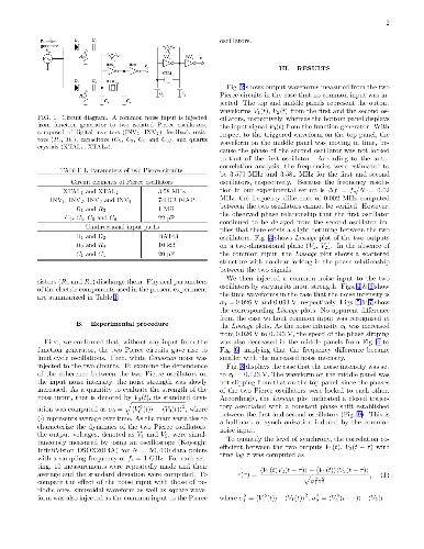
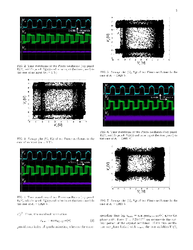
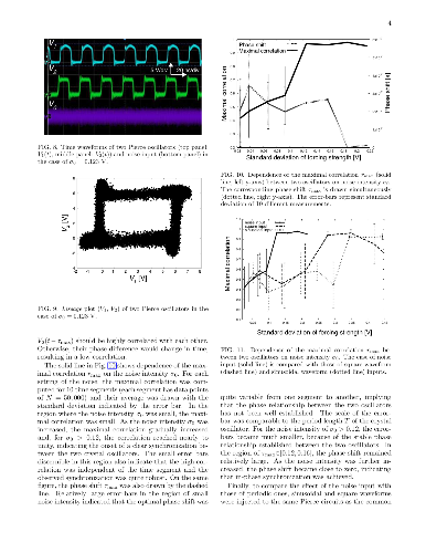
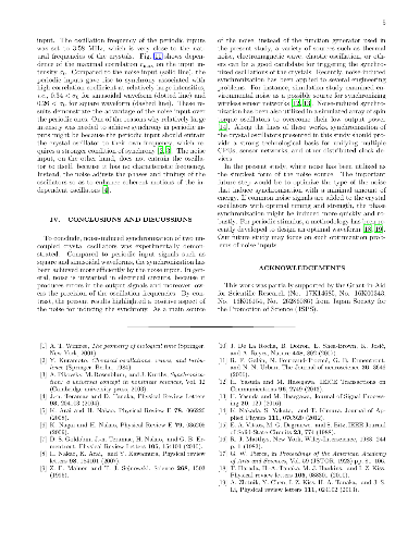
Experimental study on noise-induced synchronization of crystal oscillators is
presented. Two types of circuits were constructed: one consists of two Pierce
oscillators that were isolated from each other and received a common noise
input, while the other is based on a single Pierce oscillator that received a
same sequence of noise signal repeatedly. Due to frequency detuning between the
two Pierce oscillators, the first circuit showed no clear sign of noise-induced
synchronization. The second circuit, on the other hand, generated coherent
waveforms between different trials of the same noise injection. The waveform
coherence was, however, broken immediately after the noise injection was
terminated. Stronger modulation such as the voltage resetting was finally shown
to be effective to induce phase shifts, leading to phase-synchronization of the
Pierce oscillator. Our study presents a guideline for synchronizing clocks of
multiple CPU systems, distributed sensor networks, and other engineering
devices.
-
We present a simple and efficient Finite-Difference Time-Domain (FDFD) scheme
for simulating dispersive (Lorentz-Debye) bianisotropic metasurfaces. This
scheme replaces the conventional FDTD update equations by augmented update
equations where the effect of the metasurface, positioned at a virtual node (or
node plane) in the Yee grid, is accounted for by judiciously selected auxiliary
polarization functions, based on the Generalized Sheet Transition Conditions
(GSTCs). This scheme is computationally -- time- and memory-wise -- more
efficient and easier to implement than a previously reported scheme for
dispersive metasurfaces. It is validated in three illustrative examples.
-
Magnetic skyrmions are knot-like quasiparticles. They are candidates for
non-volatile data storage in which information is moved between fixed read and
write terminals. Read-out operation of skyrmion-based spintronic devices will
rely upon electrical detection of a single magnetic skyrmion within a
nanostructure. Here, we present Pt/Co/Ir nanodiscs which support skyrmions at
room temperature. We measured the Hall resistivity whilst simultaneously
imaging the spin texture using magnetic scanning transmission x-ray microscopy
(STXM). The Hall resistivity is correlated to both the presence and size of the
skyrmion. The size-dependent part matches the expected anomalous Hall signal
when averaging the magnetisation over the entire disc. We observed a
resistivity contribution which only depends on the number and sign of
skyrmion-like objects present in the disc. Each skyrmion gives rise to 22$\pm$2
n{\Omega} cm irrespective of its size. This contribution needs to be considered
in all-electrical detection schemes applied to skyrmion-based devices.
-
This paper deals with an inverse problem applied to the field of building
physics to experimentally estimate three sorption isotherm coefficients of a
wood fiber material. First, the mathematical model, based on convective
transport of moisture, the Optimal Experiment Design (OED) and the experimental
set-up are presented. Then measurements of relative humidity within the
material are carried out, after searching the OED, which is based on the
computation of the sensitivity functions and a priori values of the unknown
parameters employed in the mathematical model. The OED enables to plan the
experimental conditions in terms of sensor positioning and boundary conditions
out of 20 possible designs, ensuring the best accuracy for the identification
method and, thus, for the estimated parameter. Two experimental procedures were
identified: i) single step of relative humidity from 10% to 75% and ii)
multiple steps of relative humidity 10-75-33-75% with an 8-day duration period
for each step. For both experiment designs, it has been shown that the sensor
has to be placed near the impermeable boundary. After the measurements, the
parameter estimation problem is solved using an interior point algorithm to
minimize the cost function. Several tests are performed for the definition of
the cost function, by using the L^2 or L^\infty norm and considering the
experiments separately or at the same time. It has been found out that the
residual between the experimental data and the numerical model is minimized
when considering the discrete Euclidean norm and both experiments separately.
It means that two parameters are estimated using one experiment while the third
parameter is determined with the other experiment. Two cost functions are
defined and minimized for this approach. Moreover, the algorithm requires less
than 100 computations of the direct model to obtain the solution. In addition,
the OED sensitivity functions enable to capture an approximation of the
probability distribution function of the estimated parameters. The determined
sorption isotherm coefficients calibrate the numerical model to fit better the
experimental data. However, some discrepancies still appear since the model
does not take into account the hysteresis effects on the sorption capacity.
Therefore, the model is improved proposing a second differential equation for
the sorption capacity to take into account the hysteresis between the main
adsorption and desorption curves. The OED approach is also illustrated for the
estimation of five of the coefficients involved in the hysteresis model. To
conclude, the prediction of the model with hysteresis are compared with the
experimental observations to illustrate the improvement of the prediction.
-
Micro and nanomechanical resonators have been extensively researched in
recent decades for applications to time and frequency references, as well as
highly sensitive sensors. Conventionally, the operation of these resonant
sensors is practically implemented using a feedback oscillator to dynamically
track variations in the resonant frequency. However, this approach places
limitations on the frequency stability of the output response, particularly
owing to near-carrier phase noise, potentially limiting measurements over long
integration times. Here, in this paper, utilizing the recent experimental
demonstration of phononic frequency combs, we demonstrate an alternative
resonant tracking approach with the potential to provide significant
improvements in near-carrier phase noise and long-term stability. In addition,
we also showcase comb dynamics mediated resonant frequency modulation which
indirectly points to the possible control of inevitable noise processes
including thermomechanical fluctuations. This resonant tracking approach may
also have general applicability to a number of other physical oscillators.
-
A SQUID (Superconducting QUantum Interference Device) metamaterial on a Lieb
lattice with nearest-neighbor coupling supports simultaneously stable
dissipative breather families which are generated through a delicate balance of
input power and intrinsic losses. Breather multistability is possible due to
the peculiar snaking flux ampitude - frequency curve of single
dissipative-driven SQUIDs, which for relatively high sinusoidal flux field
amplitudes exhibits several stable and unstable solutions in a narrow frequency
band around resonance. These breathers are very weakly interacting with each
other, while multistability regimes with different number of simultaneously
stable breathers persist for substantial intervals of frequency, flux field
amplitude, and coupling coefficients. Moreover, the emergence of chimera states
as well as novel temporally chaotic states exhibiting spatial homogeneity
within each sublattice of the Lieb lattice is demonstrated.
-
Ultrathin planar absorbing layers, including semiconductor and metal films,
and 2D materials, are promising building blocks for solar energy harvesting
devices but poor light absorption has been a critical issue. Although
interference in ultrathin absorbing layers has been studied to realize near
perfect absorption at a specific wavelength, achieving high broadband
absorption still remains challenging. Here, we both theoretically and
experimentally demonstrated a method to tune not only reflection phase shift
but also electromagnetic energy dissipation to design broadband solar absorber
with simple planar structure consisting of an ultrathin absorbing layer
separated from the metallic substrate by a transparent layer. We explicitly
identified by deriving a new formulism that the absorbing material with
refractive index proportional to the wavelength as well as extinction
coefficient independent of the wavelength, is the ideal building block to
create ultrathin planar broadband absorbers. To demonstrate the general
strategy for naturally available absorbing materials in both high-loss
(refractory metals) and weak-absorption (2D materials) regimes, we leveraged
the bound-electron interband transition with a broad Lorentz oscillator peak to
design a solar thermal absorber based on a ultrathin Cr layer; and leveraged
the strong exciton attributed to the spin-orbit coupling for the spectrum near
the band edge, and the bound-electron interband transition for shorter
wavelengths, to design a solar photovoltaic absorber based on a atomically thin
MoS2 layer. Furthermore, our designed ultrathin broadband solar absorbers with
planar structures have comparable absorption properties compared to the
absorbers with nanopatterns. Our proposed design strategies pave the way to
novel nanometer thick energy harvesting and optoelectronic devices with simple
planar structures.
-
Transformation media theory, which steers waves in solids via an effective
geometry induced by a refractive material (Fermat's principle of least action),
provides a means of controlling vibrations and elastic waves beyond the
traditional dissipative structures regime. In particular, it could be used to
create an elastic wave cloak, shielding an interior region against elastic
waves while simultaneously preventing scattering in the outside domain.
However, as a true elastic wave cloak would generally require nonphysical
materials with stiffness tensors lacking the minor symmetry (implying
asymmetric stress), the utility of such an elastic wave cloak has thus far been
limited. Here we develop a means of overcoming this limitation via the
development of a symmetrized elastic cloak, sacrificing some of the performance
of the perfect cloak for the sake of restoring the minor symmetry. We test the
performance of the symmetrized elastic cloak for shielding a tunnel against
seismic waves, showing that it can be used to reduce the average displacement
within the tunnel by an order of magnitude (and reduce energy by two orders of
magnitude) for waves above a critical frequency of the cloak. This critical
frequency, which corresponds to the generation of surface waves at the
cloak-interior interface, can be used to develop a simple heuristic model of
the symmetrized elastic cloak's performance for a generic problem.
-
Tensor network (TN), a young mathematical tool of high vitality and great
potential, has been undergoing extremely rapid developments in the last two
decades, gaining tremendous success in condensed matter physics, atomic
physics, quantum information science, statistical physics, and so on. In this
lecture notes, we focus on the contraction algorithms of TN as well as some of
the applications to the simulations of quantum many-body systems. Starting from
basic concepts and definitions, we first explain the relations between TN and
physical problems, including the TN representations of classical partition
functions, quantum many-body states (by matrix product state, tree TN, and
projected entangled pair state), time evolution simulations, etc. These
problems, which are challenging to solve, can be transformed to TN contraction
problems. We present then several paradigm algorithms based on the ideas of the
numerical renormalization group and/or boundary states, including density
matrix renormalization group, time-evolving block decimation,
coarse-graining/corner tensor renormalization group, and several distinguished
variational algorithms. Finally, we revisit the TN approaches from the
perspective of multi-linear algebra (also known as tensor algebra or tensor
decompositions) and quantum simulation. Despite the apparent differences in the
ideas and strategies of different TN algorithms, we aim at revealing the
underlying relations and resemblances in order to present a systematic picture
to understand the TN contraction approaches.
-
Graphene oxide can be used as a precursor to graphene but the quality of
graphene flakes is highly heterogeneous. Scanning-Raman-Microscopy (SRM) is
used to characterize films of graphene derived from flakes of graphene oxide
with an almost intact carbon framework (ai-GO). The defect density of these
flakes is visualized in detail by analyzing the intensity and full-width at
half-maximum of the most pronounced Raman peaks. In addition, we superimpose
the SRM results with AFM images and correlate the spectroscopic results with
the morphology. Furthermore, we use SRM technique to display the amount of
defects in a film of graphene. Thus, an area of 250 x 250 {\my}m2 of graphene
is probed with a step-size increment of 1 {\mu}m. We are able to visualize the
position of graphene flakes, edges and the substrate. Finally, we alter
parameters of measurement to analyze the quality of graphene fast and reliable.
The described method can be used to probe and visualize the quality of graphene
films.
-
Half of the energy is always lost when charging a capacitor. Even in the
limit of vanishing resistance, half of the charging energy is still lost--to
radiation instead of heat. While this fraction can technically be reduced by
charging adiabatically, it otherwise places a fundamental limit on the charging
efficiency of a capacitor. Here we show that this 1/2 limit can be broken by
coupling a ferroelectric to the capacitor dielectric. Maxwell's equations are
solved for the coupled system to analyze energy flow from the perspective of
Poynting's theorem and show that (1) total energy dissipation is reduced below
the fundamental limit during charging and discharging; (2) energy is saved by
"recycling" the energy already stored in the ferroelectric phase transition;
and (3) this phase transition energy is directly transferred between the
ferroelectric and dielectric during charging and discharging. These results
demystify recent works on low energy negative capacitance devices as well as
lay the foundation for improving fundamental energy efficiency in all devices
that rely on energy storage in electric fields.
-
Acoustic vibrations at the nanoscale (GHz-THz frequencies) and their
interactions with electrons, photons and other excitations are the heart of an
emerging field in physics: nanophononics. The design of ultrahigh frequency
acoustic-phonon transducers, with tunable frequency, and easy to integrate in
complex systems is still an open and challenging problem for the development of
acoustic nanoscopies and phonon lasers. Here we show how an optimized plasmonic
metasurface can act as a high-frequency phonon transducer. We report pump-probe
experiments in metasurfaces composed of an array of gold nanostructures,
revealing that such arrays can act as efficient and tunable photon-phonon
transducers, with a strong spectral dependence on the excitation rate and laser
polarization. We anticipate our work to be the starting point for the
engineering of phononic metasurfaces based on plasmonic nanostructures.
-
Ultrasonic wave attenuation({\alpha}) measurement by pulse-echo method
exhibits pronounced dependence on experimental conditions. It is shown to be an
inherent characteristic of the method itself. Estimation of {\alpha} from the
component wave amplitudes in the frequency scale gives more accurate and
consistent value. This technique, viz., the Fourier Spectrum Pulse-Echo (FSPE)
is demonstrated to determine the ultrasonic velocity(v) and attenuation
constant({\alpha}) in ultrapure de-ionized water at room temperature (250C) at
1MHz and 2 MHz wave frequency.
-
Atomically thin 2-dimensional (2D) mechanical resonators are expected to be
highly sensitive force sensor and high performance nano-electro-mechanical
systems because of their excellent electrical and mechanical properties. For
practical application, the stability of their resonance frequencies against the
temperature is very crucial. Here, we demonstrate the manipulation of thermal
expansion coefficients (TECs) by making van der Waals heterojunction, graphene
and MoS2, which have opposite signs of TECs. The apparent TEC of the 2D
heterojunction is greatly suppressed to 1/3 of monolayer graphene without the
limitation of tunability of the resonance frequency by application of
electrostatic attraction.
-
Valley degrees of freedom, providing a novel way to increase the capacity and
efficiency for information storage and processing, become an important
instrumental for future photonics. However, due to the inter-valley scattering,
current realizations of the topological valley kink states are restricted to
zigzag boundaries, strongly limiting the development and applications of valley
photonics. Besides, the previous topological photonic crystals suffer from
either large thickness or insufficient electromagnetic shielding, leading to
incompatibility with the standard integrated waveguide circuits. Here, we
experimentally demonstrate the realization, engineering and manipulation of
valley-polarized topological kink states at generic boundaries in an ultrathin
substrate-integrated photonic circuitry with nearly negligible inter-valley
scattering. Valley-resolved topological kink states are manipulated by
tailoring the boundary geometry between two photonic crystals of opposite
valley Hall effects, yielding tunable edge spectrum yet robust valley-polarized
transport. Such salient properties can be exploited to design functional
substrate-integrated photonic devices, such as disorder-immune waveguides with
high transmission, robust photonic delay line, and geometry-dependent
topological channel intersections. Our systematic study provides a new route
for the manipulation of valley degrees of freedom in the substrate-integrated
circuitry, and may work as a novel integration platform for information
processing with disorder-insensitivity, easy access, and light weight.
-
Advanced electronic device technologies require a faster operation and
smaller average power consumption, which are the most important parameters in
very large scale integrated circuit design. The conventional Complementary
Metal-Oxide Semiconductor (CMOS) technology is limited by the threshold voltage
and subthreshold leakage problems in scaling of devices. This leads to failure
in adapting it to sub-micron and nanotechnologies. The carbon nanotube (CNT)
technology overcomes the threshold voltage and subthreshold leakage problems
despite reduction in size. The CNT based technology develops the most promising
devices among emerging technologies because it has most of the desired
features. Carbon Nanotube Field Effect Transistors (CNFETs) are the novel
devices that are expected to sustain the transistor scalability while
increasing its performance. Recently, there have been tremendous advances in
CNT technology for nanoelectronics applications. CNFETs avoid most of the
fundamental limitations and offer several advantages compared to silicon-based
technology. Though CNT evolves as a better option to overcome some of the bulk
CMOS problems, the CNT itself still immersed with setbacks. The fabrication of
carbon nanotube at very large digital circuits on a single substrate is
difficult to achieve. Therefore, a hybrid NP dynamic Carry Look Ahead Adder
(CLA) is designed using p-CNFET and n-MOS transistors. Here, the performance of
CLA is evaluated in 8-bit, 16-bit, 32-bit and 64-bit stages with the following
four different implementations: silicon MOSFET (Si-MOSFET) domino logic,
Si-MOSFET NP dynamic CMOS, carbon nanotube MOSFET (CN-MOSFET) domino logic, and
CN-MOSFET NP dynamic CMOS. Finally, a Hybrid CMOS-CNFET based 64-bit NP dynamic
CLA is evaluated based on HSPICE simulation in 32nm technology, which
effectively suppresses power dissipation without an increase in propagation
delay.

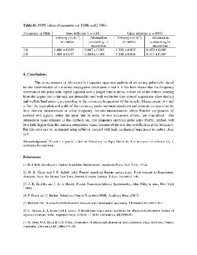
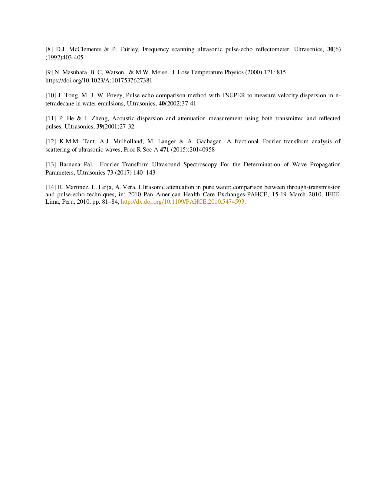
 HTS are feasible for hight power applications because of the smaller consumption demand of the cooling system in comparison to the whole power device. Real industral devices contain superconductors with 2D and 3D geometry (coated conductors tapes represent an example of 2D geometry, since the superconducting layer is very thin). In order to know the feasibility and the optimum design of a certain device, there is a need of software tools. These Numerical tools have hight requirements like fast computation, a physical model for any E(J) relation of the superconductor and any complex geometry such as coils, motors and generators, where E is the electric field and J is the current density. In this work we present a 3D variational model based on a functional that restricts the problem in the superconductor volume. We show the magnetization process of a thin film and a 3D bulk sample. We compare our model of the thin film geometry with the thin film formula, reaching a good agreement. We also compare a striated tape, where the filaments are connected by linear material, with a FEM model. We present several results for a thin film with constant critical current density, Jc, magnetic-field dependent Jc, and an anisotropic E(J) relation. For the latter, E is not parallel to J when the magnetic flux density is not perpendicular to J (force free situation). The last studied situation is the 3D cubic sample. We find the time dependence of the current density and AC loss for each situation. In the cubic bulk sample, we found a non-negligible component of the current density in the direction of the applied field. The presented numerical method is very promising for 3D modeling of superconducting samples and power applications.
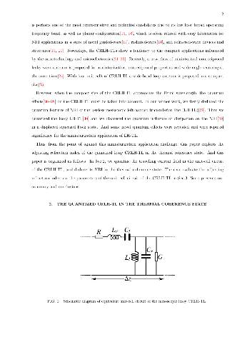
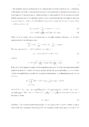
 The refraction index of the quantized lossy composite right-left handed transmission line (CRLH-TL) is deduced in the thermal coherence state. The results show that the negative refraction index (herein the left-handedness) can be implemented by the electric circuit dissipative factors(i.e., the resistances \(R\) and conductances \( G\)) in a higher frequency band (1.446GHz\(\leq\omega\leq \) 15GHz), and flexibly adjusted by the left-handed circuit components (\(C_l\), \(L_l\)) and the right-handed circuit components (\(C_r\), \(L_r\)) at a lower frequency (\(\omega\)=0.995GHz) . The flexible adjustment for left-handedness in a wider bandwidth will be significant for the microscale circuit design of the CRLH-TL and may make the theoretical preparation for its compact applications.
 Experimental study on noise-induced synchronization of crystal oscillators is presented. Two types of circuits were constructed: one consists of two Pierce oscillators that were isolated from each other and received a common noise input, while the other is based on a single Pierce oscillator that received a same sequence of noise signal repeatedly. Due to frequency detuning between the two Pierce oscillators, the first circuit showed no clear sign of noise-induced synchronization. The second circuit, on the other hand, generated coherent waveforms between different trials of the same noise injection. The waveform coherence was, however, broken immediately after the noise injection was terminated. Stronger modulation such as the voltage resetting was finally shown to be effective to induce phase shifts, leading to phase-synchronization of the Pierce oscillator. Our study presents a guideline for synchronizing clocks of multiple CPU systems, distributed sensor networks, and other engineering devices.

 This paper deals with an inverse problem applied to the field of building physics to experimentally estimate three sorption isotherm coefficients of a wood fiber material. First, the mathematical model, based on convective transport of moisture, the Optimal Experiment Design (OED) and the experimental set-up are presented. Then measurements of relative humidity within the material are carried out, after searching the OED, which is based on the computation of the sensitivity functions and a priori values of the unknown parameters employed in the mathematical model. The OED enables to plan the experimental conditions in terms of sensor positioning and boundary conditions out of 20 possible designs, ensuring the best accuracy for the identification method and, thus, for the estimated parameter. Two experimental procedures were identified: i) single step of relative humidity from 10% to 75% and ii) multiple steps of relative humidity 10-75-33-75% with an 8-day duration period for each step. For both experiment designs, it has been shown that the sensor has to be placed near the impermeable boundary. After the measurements, the parameter estimation problem is solved using an interior point algorithm to minimize the cost function. Several tests are performed for the definition of the cost function, by using the L^2 or L^\infty norm and considering the experiments separately or at the same time. It has been found out that the residual between the experimental data and the numerical model is minimized when considering the discrete Euclidean norm and both experiments separately. It means that two parameters are estimated using one experiment while the third parameter is determined with the other experiment. Two cost functions are defined and minimized for this approach. Moreover, the algorithm requires less than 100 computations of the direct model to obtain the solution. In addition, the OED sensitivity functions enable to capture an approximation of the probability distribution function of the estimated parameters. The determined sorption isotherm coefficients calibrate the numerical model to fit better the experimental data. However, some discrepancies still appear since the model does not take into account the hysteresis effects on the sorption capacity. Therefore, the model is improved proposing a second differential equation for the sorption capacity to take into account the hysteresis between the main adsorption and desorption curves. The OED approach is also illustrated for the estimation of five of the coefficients involved in the hysteresis model. To conclude, the prediction of the model with hysteresis are compared with the experimental observations to illustrate the improvement of the prediction.
 Tensor network (TN), a young mathematical tool of high vitality and great potential, has been undergoing extremely rapid developments in the last two decades, gaining tremendous success in condensed matter physics, atomic physics, quantum information science, statistical physics, and so on. In this lecture notes, we focus on the contraction algorithms of TN as well as some of the applications to the simulations of quantum many-body systems. Starting from basic concepts and definitions, we first explain the relations between TN and physical problems, including the TN representations of classical partition functions, quantum many-body states (by matrix product state, tree TN, and projected entangled pair state), time evolution simulations, etc. These problems, which are challenging to solve, can be transformed to TN contraction problems. We present then several paradigm algorithms based on the ideas of the numerical renormalization group and/or boundary states, including density matrix renormalization group, time-evolving block decimation, coarse-graining/corner tensor renormalization group, and several distinguished variational algorithms. Finally, we revisit the TN approaches from the perspective of multi-linear algebra (also known as tensor algebra or tensor decompositions) and quantum simulation. Despite the apparent differences in the ideas and strategies of different TN algorithms, we aim at revealing the underlying relations and resemblances in order to present a systematic picture to understand the TN contraction approaches.
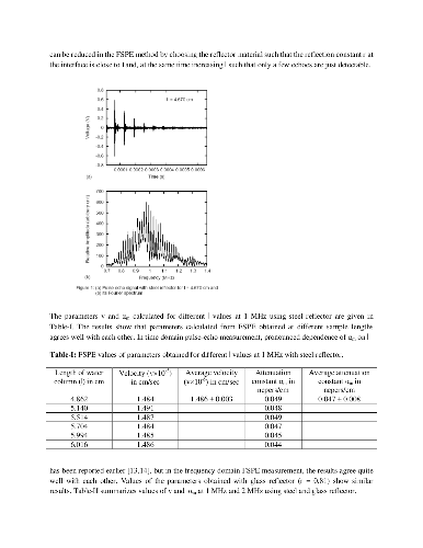
 Ultrasonic wave attenuation({\alpha}) measurement by pulse-echo method exhibits pronounced dependence on experimental conditions. It is shown to be an inherent characteristic of the method itself. Estimation of {\alpha} from the component wave amplitudes in the frequency scale gives more accurate and consistent value. This technique, viz., the Fourier Spectrum Pulse-Echo (FSPE) is demonstrated to determine the ultrasonic velocity(v) and attenuation constant({\alpha}) in ultrapure de-ionized water at room temperature (250C) at 1MHz and 2 MHz wave frequency.