-
For a regular cardinal κ, a formula of the modal μ-calculus is
κ-continuous in a variable x if, on every model, its interpretation as a
unary function of x is monotone and preserves unions of κ-directed sets.
We define the fragment Cℵ1(x) of the modal μ-calculus and prove
that all the formulas in this fragment are ℵ1-continuous. For each
formula ϕ(x) of the modal μ-calculus, we construct a formula ψ(x)∈Cℵ1(x) such that ϕ(x) is κ-continuous, for some
κ, if and only if ϕ(x) is equivalent to ψ(x). Consequently, we
prove that (i) the problem whether a formula is κ-continuous for some
κ is decidable, (ii) up to equivalence, there are only two fragments
determined by continuity at some regular cardinal: the fragment
Cℵ0(x) studied by Fontaine and the fragment Cℵ1(x). We
apply our considerations to the problem of characterizing closure ordinals of
formulas of the modal μ-calculus. An ordinal α is the closure
ordinal of a formula ϕ(x) if its interpretation on every model converges
to its least fixed-point in at most α steps and if there is a model
where the convergence occurs exactly in α steps. We prove that
ω1, the least uncountable ordinal, is such a closure ordinal. Moreover
we prove that closure ordinals are closed under ordinal sum. Thus, any formal
expression built from 0, 1, ω, ω1 by using the binary operator
symbol + gives rise to a closure ordinal.
-
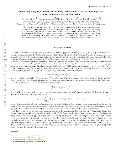
We show that dyon and magnetic monopole can be constructed in the
gauge-independent way for the SU(2) Yang--Mills theory even in the absence of
the scalar field. This result is derived from the recent proposal for obtaining
non-trivial topological configurations responsible for quark confinement in the
Yang-Mills theory based on the Confinement-Higgs complementary relationship
between the pure Yang-Mills theory and the gauge-scalar model with an adjoint
scalar field of the fixed length. We discuss how such configurations have the
implications for quark confinement.
-
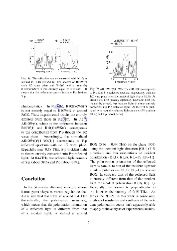
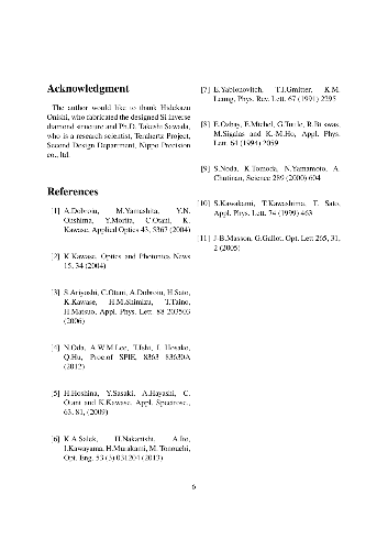
The band structure of an Si inverse diamond structure whose lattice point
shape was vacant regular octahedrons, was calculated using plane wave expansion
method. A complete photonic band gap was theoretically confirmed at around 0.4
THz. It is said that three-dimensional photonic crystals have no polarization
anisotropy in photonic band gap (stop gap, stop band) of high symmetry points
in normal incidence. However, it was experimentally confirmed that the
polarization orientation of a reflected wave was different from that of an
incident wave, [I(X,Y)], where (X,Y) is the coordinate system fixed in the
photonic crystal. It was studied on a plane (001) at around X point's photonic
band gap (0.36 − 0.44 THz) for incident wave direction [001] by rotating a
sample in the plane (001), relatively. The polarization orientation of the
reflected wave was parallel to that of the incident wave when that of the
incident wave was I(1, 1) or I(1, −1). In contrast, the former was
perpendicular to the latter when that of the incident wave was I(1, 0) or I(0,
−1) at around 0.38 THz. As far as the photonic crystal in this work is
concerned, method of resolution and synthesis of the incident polarization
vector is not able to apply to the analyses of rotation of the measured
reflected spectra in appearance.
-
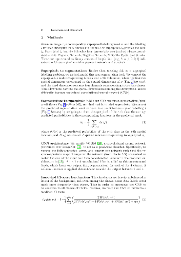
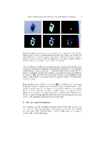
The presence of certain clinical dermoscopic features within a skin lesion
may indicate melanoma, and automatically detecting these features may lead to
more quantitative and reproducible diagnoses. We reformulate the task of
classifying clinical dermoscopic features within superpixels as a segmentation
problem, and propose a fully convolutional neural network to detect clinical
dermoscopic features from dermoscopy skin lesion images. Our neural network
architecture uses interpolated feature maps from several intermediate network
layers, and addresses imbalanced labels by minimizing a negative multi-label
Dice-F1 score, where the score is computed across the mini-batch for each
label. Our approach ranked first place in the 2017 ISIC-ISBI Part 2:
Dermoscopic Feature Classification Task challenge over both the provided
validation and test datasets, achieving a 0.895% area under the receiver
operator characteristic curve score. We show how simple baseline models can
outrank state-of-the-art approaches when using the official metrics of the
challenge, and propose to use a fuzzy Jaccard Index that ignores the empty set
(i.e., masks devoid of positive pixels) when ranking models. Our results
suggest that (i) the classification of clinical dermoscopic features can be
effectively approached as a segmentation problem, and (ii) the current metrics
used to rank models may not well capture the efficacy of the model. We plan to
make our trained model and code publicly available.
-
We revisit the manifestly covariant large c expansion of General
Relativity, c being the speed of light. Assuming the relativistic connection
has no pole in c−2, this expansion is known to reproduce Newton-Cartan
gravity and a covariant version of Post-Newtonian corrections to it. We show
that relaxing this assumption leads to the inclusion of twistless torsion in
the effective non-relativistic theory. We argue that the resulting TTNC theory
is an effective description of a non-relativistic regime of General Relativity
that extends Newtonian physics by including strong gravitational time dilation.
-
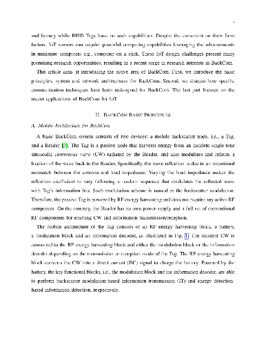
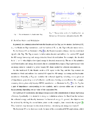
The rapid growth of IoT driven by recent advancements in consumer
electronics, 5G communication technologies, and cloud-computing enabled
big-data analytics, has recently attracted tremendous attention from both the
industry and academia. One of the major open challenges for IoT is the limited
network lifetime due to massive IoT devices being powered by batteries with
finite capacities. The low-power and low-complexity backscatter communications
(BackCom), which simply relies on passive reflection and modulation of an
incident radio-frequency (RF) wave, has emerged to be a promising technology
for tackling this challenge. However, the contemporary BackCom has several
major limitations, such as short transmission range, low data rate, and
uni-directional information transmission. The article aims at introducing the
recent advances in the active area of BackCom. Specifically, we provide a
systematic introduction of the next generation BackCom covering basic
principles, systems, techniques besides IoT applications. Lastly, we describe
the IoT application scenarios with the next generation BackCom.
-
We prove that square-tiled surfaces having fixed combinatorics of horizontal
cylinder decomposition and tiled with smaller and smaller squares become
asymptotically equidistributed in any ambient linear GL(R)-invariant
suborbifold defined over Q in the moduli space of Abelian
differentials. Moreover, we prove that the combinatorics of the horizontal and
of the vertical decompositions are asymptotically uncorrelated. As a
consequence, we prove the existence of an asymptotic distribution for the
combinatorics of a "random" interval exchange transformation with integer
lengths.
We compute explicitly the absolute contribution of square-tiled surfaces
having a single horizontal cylinder to the Masur-Veech volume of any ambient
stratum of Abelian differentials. The resulting count is particularly simple
and efficient in the large genus asymptotics. We conjecture that the
corresponding relative contribution is asymptotically of the order 1/d, where
d is the dimension of the stratum, and prove that this conjecture is
equivalent to the long-standing conjecture on the large genus asymptotics of
the Masur-Veech volumes. We prove, in particular, that the recent results of
Chen, M\"oller and Zagier imply that the conjecture holds for the principal
stratum of Abelian differentials as the genus tends to infinity.
Our result on random interval exchanges with integer lengths allows to make
empirical computation of the probability to get a 1-cylinder pillowcase cover
taking a "random" one in a given stratum. We use this technique to derive the
approximate values of the Masur-Veech volumes of strata of quadratic
differentials of all small dimensions.
-
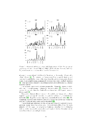
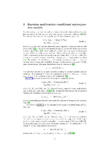
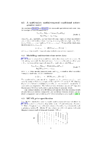
It is well recognised that animal and plant pathogens form complex ecological
communities of interacting organisms within their hosts. Although community
ecology approaches have been applied to determine pathogen interactions at the
within-host scale, methodologies enabling robust inference of the
epidemiological impact of pathogen interactions are lacking. Here we developed
a novel statistical framework to identify statistical covariances from the
infection time-series of multiple pathogens simultaneously. Our framework
extends Bayesian multivariate disease mapping models to analyse multivariate
time series data by accounting for within- and between-year dependencies in
infection risk and incorporating a between-pathogen covariance matrix which we
estimate. Importantly, our approach accounts for possible confounding drivers
of temporal patterns in pathogen infection frequencies, enabling robust
inference of pathogen-pathogen interactions. We illustrate the validity of our
statistical framework using simulated data and applied it to diagnostic data
available for five respiratory viruses co-circulating in a major urban
population between 2005 and 2013: adenovirus, human coronavirus, human
metapneumovirus, influenza B virus and respiratory syncytial virus. We found
positive and negative covariances indicative of epidemiological interactions
among specific virus pairs. This statistical framework enables a community
ecology perspective to be applied to infectious disease epidemiology with
important utility for public health planning and preparedness.
-
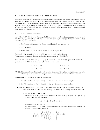
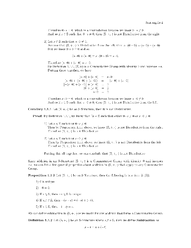
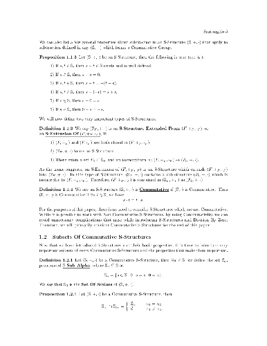
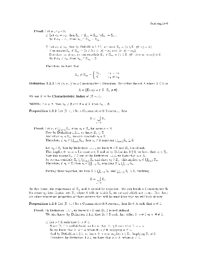
To allow for Division By Zero, we develop a new algebraic structure
containing addition and multiplication called an S-Extension of a Field. This
unique structure extends a Field so that the equation 0⋅s=x has exactly
one solution for every non-zero Field element x. Furthermore, a different
solution is obtained for each choice of x, making this solution unique to
that particular equation. However, the equation 0⋅s=0 has two or more
solutions, with no preference towards any one particular solution. This allows
us to use the usual definition of division as the solution to the equation
0⋅s=x to evaluate x divided by 0. And if x≠0, every x0 is a unique element that is also unique to that particular x while
00 remains indeterminate. This creates a Division By Zero which
significantly differs from other attempts at Division By Zero.
-
The complex method of interpolation, going back to Calder\'on and Coifman et
al., on the one hand, and the Alexander-Wermer-Slodkowski theorem on polynomial
hulls with convex fibers, on the other hand, are generalized to a method of
interpolation of real (finite-dimensional) Banach spaces and of convex
functions. The underlying duality in this method is given by the Legendre
transform. Our results can also be interpreted as new properties of solutions
of the homogeneous complex Monge-Amp\`ere equation.
-
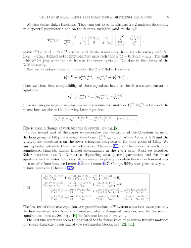
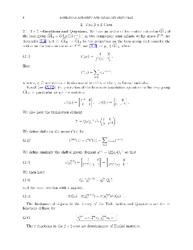
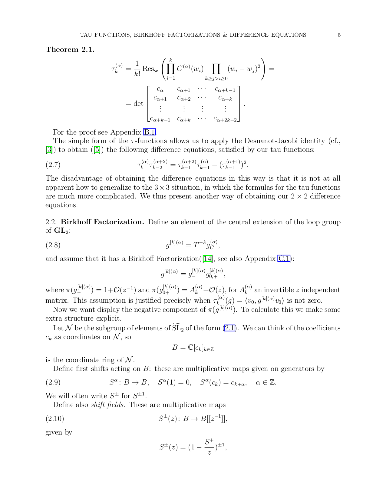
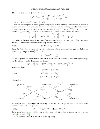
Q-systems and T-systems are systems of integrable difference equations
that have recently attracted much attention, and have wide applications in
representation theory and statistical mechanics. We show that certain
τ-functions, given as matrix elements of the action of the loop group of
GL2 on two-component fermionic Fock space, give solutions of a
Q-system. An obvious generalization using the loop group of GL3
acting on three-component fermionic Fock space leads to a new system of 4
difference equations.
-
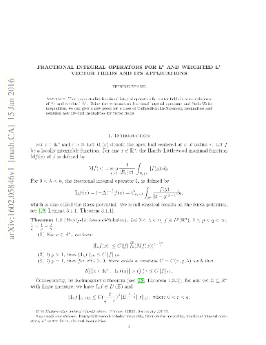
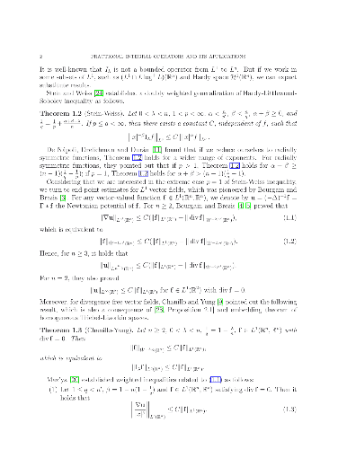
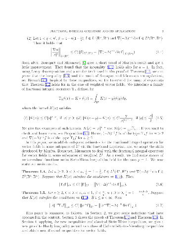
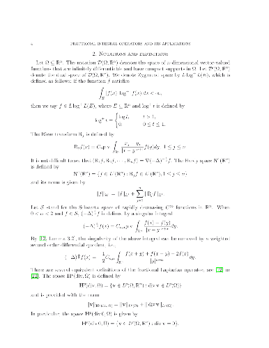
This paper studies fractional integral operator for vector fields in weighted
L1. Using the estimates on fractional integral operator and Stein-Weiss
inequalities, we can give a new proof for a class of Caffarelli-Kohn-Nirenberg
inequalities and establish new \divg-\curl inequalities for vector fields.
-
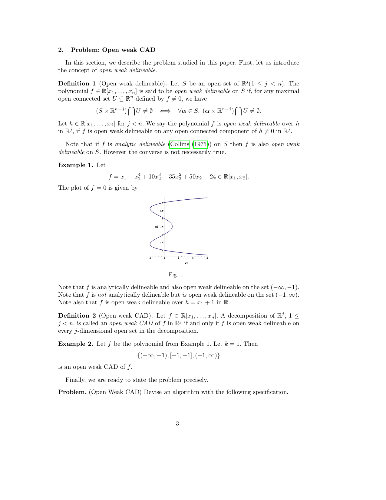
The concept of open weak CAD is introduced. Every open CAD is an open weak
CAD. On the contrary, an open weak CAD is not necessarily an open CAD. An
algorithm for computing projection polynomials of open weak CADs is proposed.
The key idea is to compute the intersection of projection factor sets produced
by different projection orders. The resulting open weak CAD often has smaller
number of sample points than open CADs. The algorithm can be used for computing
sample points for all open connected components of f≠0 for a given
polynomial f. It can also be used for many other applications, such as
testing semi-definiteness of polynomials and copositive problems. In fact, we
solved several difficult semi-definiteness problems efficiently by using the
algorithm. Furthermore, applying the algorithm to copositive problems, we find
an explicit expression of the polynomials producing open weak CADs under some
conditions, which significantly improves the efficiency of solving copositive
problems.
-
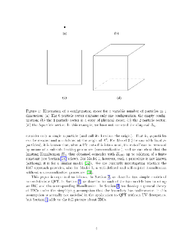
We propose a way of defining Hamiltonians for quantum field theories without
any renormalization procedure. The resulting Hamiltonians, called IBC
Hamiltonians, are mathematically well-defined (and in particular, ultraviolet
finite) without an ultraviolet cut-off such as smearing out the particles over
a nonzero radius; rather, the particles are assigned radius zero. These
Hamiltonians agree with those obtained through renormalization whenever both
are known to exist. We describe explicit examples of IBC Hamiltonians. Their
definition, which is best expressed in the particle-position representation of
the wave function, involves a kind of boundary condition on the wave function,
which we call an interior-boundary condition (IBC). The relevant configuration
space is one of a variable number of particles, and the relevant boundary
consists of the configurations with two or more particles at the same location.
The IBC relates the value (or derivative) of the wave function at a boundary
point to the value of the wave function at an interior point (here, in a sector
of configuration space corresponding to a lesser number of particles).
-
This work contains a proof of a non-trivial explicit quantitative bound in
the eigenvalue aspect for the sup-norm of a SL(3,Z) Hecke-Maass cusp form
restricted to a compact set.
-
A C*-dynamical system is said to have the ideal separation property if every
ideal in the corresponding crossed product arises from an invariant ideal in
the C*-algebra. In this paper we characterize this property for unital
C*-dynamical systems over discrete groups. To every C*-dynamical system we
associate a "twisted" partial C*-dynamical system that encodes much of the
structure of the action. This system can often be "untwisted," for example when
the algebra is commutative, or when the algebra is prime and a certain specific
subgroup has vanishing Mackey obstruction. In this case, we obtain relatively
simple necessary and sufficient conditions for the ideal separation property. A
key idea is a notion of noncommutative boundary for a C*-dynamical system that
generalizes Furstenberg's notion of topological boundary for a group.
-
The Tur\'an function ex(n,F) denotes the maximal number of edges in an
F-free graph on n vertices. We consider the function hF(n,q), the
minimal number of copies of F in a graph on n vertices with ex(n,F)+q
edges. The value of hF(n,q) has been extensively studied when F is
bipartite or colour-critical. In this paper we investigate the simplest
remaining graph F, namely, two triangles sharing a vertex, and establish the
asymptotic value of hF(n,q) for q=o(n2).
-
We investigate the universal cover of a topological group that is not
necessarily connected. Its existence as a topological group is governed by a
Taylor cocycle, an obstruction in 3-cohomology. Alternatively, it always exists
as a topological 2-group. The splitness of this 2-group is also governed by an
obstruction in 3-cohomology, a Sinh cocycle. We give explicit formulas for both
obstructions and show that they are inverse of each other.
-
Semidefinite programs (SDPs) -- some of the most useful and versatile
optimization problems of the last few decades -- are often pathological: the
optimal values of the primal and dual problems may differ and may not be
attained. Such SDPs are both theoretically interesting and often impossible to
solve; yet, the pathological SDPs in the literature look strikingly similar.
Based on our recent work \cite{Pataki:17} we characterize pathological
semidefinite systems by certain {\em excluded matrices}, which are easy to spot
in all published examples. Our main tool is a normal (canonical) form of
semidefinite systems, which makes their pathological behavior easy to verify.
The normal form is constructed in a surprisingly simple fashion, using mostly
elementary row operations inherited from Gaussian elimination. The proofs are
elementary and can be followed by a reader at the advanced undergraduate level.
As a byproduct, we show how to transform any linear map acting on symmetric
matrices into a normal form, which allows us to quickly check whether the image
of the semidefinite cone under the map is closed. We can thus introduce readers
to a fundamental issue in convex analysis: the linear image of a closed convex
set may not be closed, and often simple conditions are available to verify the
closedness, or lack of it.
-
Tensor hierarchies are algebraic objects that emerge in gauging procedures in
supergravity models, and that present a very deep and intricate relationship
with Leibniz (or Loday) algebras. In this paper, we show that one can
canonically associate a tensor hierarchy to any Loday algebra. By formalizing
the construction that is performed in supergravity, we build this tensor
hierarchy explicitly. We show that this tensor hierarchy can be canonically
equipped with a differential graded Lie algebra structure that coincides with
the one that is found in supergravity theories.
-
In the genomic era, the identification of gene signatures associated with
disease is of significant interest. Such signatures are often used to predict
clinical outcomes in new patients and aid clinical decision-making. However,
recent studies have shown that gene signatures are often not replicable. This
occurrence has practical implications regarding the generalizability and
clinical applicability of such signatures. To improve replicability, we
introduce a novel approach to select gene signatures from multiple datasets
whose effects are consistently non-zero and account for between-study
heterogeneity. We build our model upon some rank-based quantities, facilitating
integration over different genomic datasets. A high dimensional penalized
Generalized Linear Mixed Model (pGLMM) is used to select gene signatures and
address data heterogeneity. We compare our method to some commonly used
strategies that select gene signatures ignoring between-study heterogeneity. We
provide asymptotic results justifying the performance of our method and
demonstrate its advantage in the presence of heterogeneity through thorough
simulation studies. Lastly, we motivate our method through a case study
subtyping pancreatic cancer patients from four gene expression studies.
-
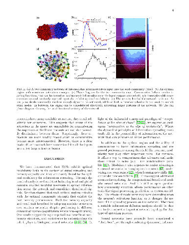
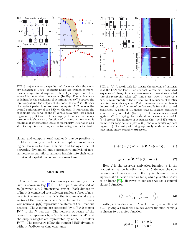
The neural network is a powerful computing framework that has been exploited
by biological evolution and by humans for solving diverse problems. Although
the computational capabilities of neural networks are determined by their
structure, the current understanding of the relationships between a neural
network's architecture and function is still primitive. Here we reveal that
neural network's modular architecture plays a vital role in determining the
neural dynamics and memory performance of the network of threshold neurons. In
particular, we demonstrate that there exists an optimal modularity for memory
performance, where a balance between local cohesion and global connectivity is
established, allowing optimally modular networks to remember longer. Our
results suggest that insights from dynamical analysis of neural networks and
information spreading processes can be leveraged to better design neural
networks and may shed light on the brain's modular organization.
-
We propose a general framework for nonasymptotic covariance matrix estimation
making use of concentration inequality-based confidence sets. We specify this
framework for the estimation of large sparse covariance matrices through
incorporation of past thresholding estimators with key emphasis on support
recovery. This technique goes beyond past results for thresholding estimators
by allowing for a wide range of distributional assumptions beyond merely
sub-Gaussian tails. This methodology can furthermore be adapted to a wide range
of other estimators and settings. The usage of nonasymptotic dimension-free
confidence sets yields good theoretical performance. Through extensive
simulations, it is demonstrated to have superior performance when compared with
other such methods. In the context of support recovery, we are able to specify
a false positive rate and optimize to maximize the true recoveries.
-
Recently representation theory has been used to provide atomic decompositions
for a large collection of classical Banach spaces. In this paper we extend the
techniques to also include projective representations. As our main application
we obtain atomic decompositions of Bergman spaces on the unit ball through the
holomorphic discrete series for the group of isometries of the ball.
-
This article proves that an irreducible subfactor planar algebra with a
distributive biprojection lattice admits a minimal 2-box projection generating
the identity biprojection. It is a generalization (conjectured in 2013) of a
theorem of Oystein Ore on distributive intervals of finite groups (1938), and a
corollary of a natural subfactor extension of a conjecture of Kenneth S. Brown
in algebraic combinatorics (2000). We deduce a link between combinatorics and
representations in finite group theory.